Build Your Own Clone Message Board

It is currently Sun Apr 28, 2024 2:05 am

All times are UTC - 6 hours


Post new topic Reply to topic  [ 26 posts ]  Go to page 1, 2  Next
Author Message
PostPosted: Mon Jul 28, 2014 12:26 pm 
Offline

Joined: Thu Jul 24, 2014 6:03 am
Posts: 17
Hello!

First of all, I will try to explain me in the best manner, but forgive me if I won't because I'm not enough good in english as I would like to be (I'm from Spain).

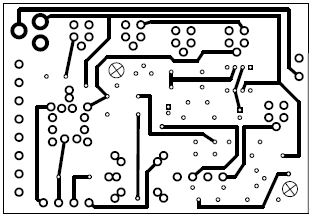
I wasn't able to buy the drop-in PCB from BYOC store because the shipping costs were too high, so I decided to do a complete DIY project and made my own PCB. I copied the design of the top layer from a picture that BYOC use to announce their dop-in kit, but I didn't find any "official" picture of the bottom layer, and I used one that I found in Internet:

Attachment:
Bottom layer.jpg
Bottom layer.jpg [ 146.03 KiB | Viewed 11373 times ]


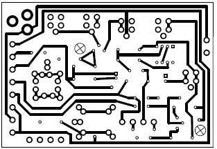
And finally, I had these designs for the layers, top and bottom respectively:

Attachment:
Top layer design.JPG
Top layer design.JPG [ 28.01 KiB | Viewed 11373 times ]

Attachment:
Bottom layer design.JPG
Bottom layer design.JPG [ 30.71 KiB | Viewed 11374 times ]


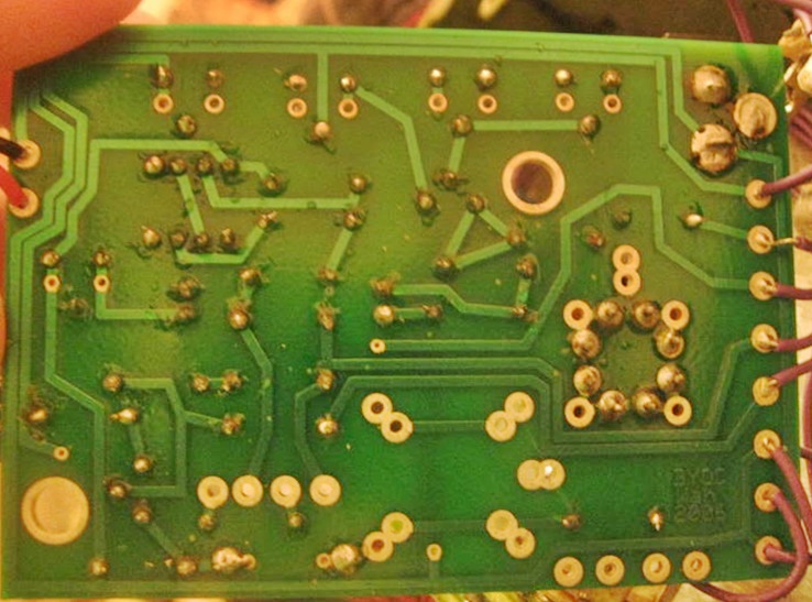
I don't know if it's not working due to a bad design on the bottom layer, but what I know is that the original PCB has plated eyelets that makes a connection between top and bottom layer, and I've done this connection by soldering a very short cable from top to bottom layer (except with resistors and capacitors, which I've could weld directly to the pad), in the cases that is needed to connect both layers (namely, when a copper track from the bottom layer and other one from the top layer arrives to the same eyelet).

When I plugged my guitar to the stereo input and the amplifier to the mono output, I turned on my amp and push the footswitch and the first thing I saw was the LED on, and what I heard were a pop (I think that the pop's should be avoided if I use the 3PDT wiring that Stephen says in the 5th diagram of this thread...: viewtopic.php?f=9&t=6525 ), and when I increased the volume pot of my guitar, I saw that the luminosity of the LED decreased, and I didn't heard sound. Also, I hear that, when I was increasing and decreasing the volume pot of the guitar, the amp amplifies that sound, I mean: Like when a potentiometer has some powder inside and you hear in some moment how the variable resistor moves that powder.

This is a list of things that I've already do:

- Weld again all the non-superbrilliant weldings of the bottom layer.
- Ensure that all components are in the right place (they are).
- Ensure that the wiring is correctly like Stephen says in the topic that I was referring before, and like the BYOC instructions.

After this, I've tried again the pedal and the only thing that has changed is that there's no pops when I turn on and off the pedal, but in bypass mode, I listen a high frequency linear sound (I think it's a G, if the note means something...), and when I turn on, the volume of that sound decreases a little bit.

I know that the pictures you will see below are not in good quality, so here are the colours that I've used and for what:

VIOLET: From IN of the PCB to pin 5 of 3PDT.

BLUE: From OUT of the PCB to pin 7 of 3PDT.

GREEN: From "jack" pads to the sleeves of the jack's.

ORANGE, WHITE AND BROWN: From 1, 2, 3 named pads to the 1, 2 and 3 lugs of the ICAR pot, respectively.

GREY: - From pin 1 to a 1k resistor, which is connected to the LED
- From "ring" pad to ring lug of the stereo jack input.
- From the non-commoun pad of gain and Q pots to the non-comoun lug of the pots.

YELLOW: From pin 4 to stereo jack tip (input) and from the pin 8 to mono jack tip (output).

RED: - From the +9V battery pad to the LED, and to the positive cable of the battery clip.
- From the commoun pad of gain and Q pots to the commoun lug of the pots.

BLACK: - From pin 2 to the sleeve of the stereo jack.
- From pin 4 to pin 9.
- From pint 3 to pin 6.
- From negative pad of the battery to the negative cable of the battery clip.

I can only attach 3 images, so in the post below I will attach the photos.

And one last thing.. I didn't use 0 ohm resistors... Can be this the reason? I think that a cable is the same...

Hope you help me, I've spent A LOT of time with this pedal and I think that I can make it works..

Thank you!


Javi.


Last edited by JaviSixStrings on Mon Jul 28, 2014 12:32 pm, edited 2 times in total.

Top
 Profile  
 
PostPosted: Mon Jul 28, 2014 12:28 pm 
Offline

Joined: Thu Jul 24, 2014 6:03 am
Posts: 17
Attachment:
Top layer.jpg
Top layer.jpg [ 632 KiB | Viewed 11373 times ]


Attachment:
Bottom layer.jpg
Bottom layer.jpg [ 663.34 KiB | Viewed 11373 times ]


Attachment:
Wiring.jpg
Wiring.jpg [ 743.29 KiB | Viewed 11373 times ]


Top
 Profile  
 
PostPosted: Mon Jul 28, 2014 1:58 pm 
Offline
Moderator
User avatar

Joined: Sat Mar 04, 2006 9:15 pm
Posts: 7662
Location: Ohio
Use the image and diagram below along with a continuity checker to confirm all of your connections from component to component.

Image
Image

_________________
"It’s your soldering."


Top
 Profile  
 
PostPosted: Tue Jul 29, 2014 7:00 am 
Offline

Joined: Thu Jul 24, 2014 6:03 am
Posts: 17
All components are conected like the schematic without any resistance, except the 0.01uF range cap to the halo inductor, that have 95.5kOhms (from both extremes of the inductor), but I don't see any cooper track connected directly between two components...


Top
 Profile  
 
PostPosted: Tue Jul 29, 2014 8:15 am 
Offline
Moderator
User avatar

Joined: Sat Mar 04, 2006 9:15 pm
Posts: 7662
Location: Ohio
It could be an issue with your soldering. I see what looks to be several cold solder joints but the photo is so blurry it’s hard to say with any certainty.

_________________
"It’s your soldering."


Top
 Profile  
 
PostPosted: Tue Jul 29, 2014 8:32 am 
Offline

Joined: Thu Jul 24, 2014 6:03 am
Posts: 17
I will weld again the top layer pads... Nevertheless, if you zoom the web page to 25%, I think that the quality is better.

On the other hand, it's not due to the zero ohm resistors, right? And that measure of 95.5kOhms it's correct?

Thank you!


Top
 Profile  
 
PostPosted: Tue Jul 29, 2014 9:48 am 
Offline
Moderator
User avatar

Joined: Sat Mar 04, 2006 9:15 pm
Posts: 7662
Location: Ohio
You definitely have a problem with that 95.5K ohm reading. If you are measuring from the correct places you should have continuity (no resistance) between the left side of C5 as shown in the schematic and the right side of the inductor. When I measure from the left side of C5 to the opposite side of the inductor I only get 14.7Ω

_________________
"It’s your soldering."


Top
 Profile  
 
PostPosted: Tue Jul 29, 2014 11:02 am 
Offline

Joined: Thu Jul 24, 2014 6:03 am
Posts: 17
Can you tell me if these two pads are connected?

Attachment:
Bottom layer soldering question.jpg
Bottom layer soldering question.jpg [ 146.58 KiB | Viewed 11349 times ]


I think that's the only manner to have continuity between the left side of C5 and the lower extreme of the inductor (which is connected to the zero ohm resistor, because only the inductor already has 27 ohms of resistance, so I think that you're referring to the lower extreme by saying "right side of the inductor", correct me if it's not, please).

I've put a jumper between left side of C5 and right side of zero ohm resistor, and I get continuity (2 ohm more or less)...

I've been searching other forms to connect these two components (C5-left side and inductor-lower extreme), but, seriously, I haven't been able to find any more forms, if they exist..


Top
 Profile  
 
PostPosted: Tue Jul 29, 2014 11:39 am 
Offline
Moderator
User avatar

Joined: Sat Mar 04, 2006 9:15 pm
Posts: 7662
Location: Ohio
Someone with a BYOC PCB in their wah will have to answer your solder pad continuity question. I’ve got a self etched copy of the Dunlop PCB in my pedal.

_________________
"It’s your soldering."


Top
 Profile  
 
PostPosted: Tue Jul 29, 2014 1:14 pm 
Offline

Joined: Thu Jul 24, 2014 6:03 am
Posts: 17
Okay, but, do you know if I will break some component if I try the pedal like I said? I think that there isn't enough intensity to break the resistors or the caps... But I wanna be sure.

Thanks a lot, Stephen :-)


Top
 Profile  
 
PostPosted: Tue Jul 29, 2014 2:10 pm 
Offline
Moderator
User avatar

Joined: Sat Mar 04, 2006 9:15 pm
Posts: 7662
Location: Ohio
I can’t see how any damage could occur if you shorted the two solder pads together.

_________________
"It’s your soldering."


Top
 Profile  
 
PostPosted: Wed Jul 30, 2014 6:16 am 
Offline

Joined: Thu Jul 24, 2014 6:03 am
Posts: 17
Anything has changed...

In bypass mode, I still listen the high frequency sound and all parameters make their purpose over that sound (bass and mids trimpots and gains and Q pots) except the buffer volume trimpot. When I push the switch, the sound changes into a low frequency sound (with a far away part of high frequency) and the effect of the parameters over the sounds are less relevant.

That occurs whether I put or not the jumper I said before (between C5 left side and inductor lower extreme). I've been searching, again, other form to connect these two components, but I haven't found it...

Other thing I can assure is that the transistor Q1 is in the cut-off region of operation, and I don't know why.. (well, I know why theoretically, but not sure if this is the region where it should actually be).

I've already welded again ALL pads (they're all brilliants), I've checked all connections between components (the only connection that don't give me a continuity lecture is which I said before, between C5 left side and inductor lower extreme) for second time, and I checked the wiring and the connections between all external components (from PCB to 3PDT and input and output jack) for second time too.

I don't know what more I can do... :cry: I only want it to sound, even if it's a bad sound.. If it's bad, then I will have the chance to make it sounds better, but now... I cannot...

I'm going to ask for a good quality camera and shoot good pictures. It will help you in order to help me, thinking in what I said before? I remind you, BYOC forum, that the principal difference between my BYOC wah and, I think, most of other BYOC wah is that I've built the PCB from zero, making the design of the top layer from an "official" picture and the bottom layer (which I think that maybe has an error in some copper track) from a picture that I found on internet...

Hope you help me guys...

Thanks!

P.S: Sorry if there's any bad expression, I've wrote it a little bit quickly.


Top
 Profile  
 
PostPosted: Tue Aug 05, 2014 9:50 am 
Offline

Joined: Thu Jul 24, 2014 6:03 am
Posts: 17
Hello again.

I've fixed the error that had my PCB. I've checked again the continuity between all components as is shown in the schematic and all it's okay.

I think that all the wiring its okay, I've checked it for the third time...

When I turn on the wah, there's no sound through the amp, and when I turn it off, I can hear a high frequency sound, and if I move the potentiometers and the trim pots, that sound changes according to the parameter that I change. I don't understand that, because if it's in bypass mode, I thought that anything of the pedal must change the sound... As you can see, there's a LED connected that indicates me if it's ON or OFF (and yes, I've connected correctly the LED). Also, when I move the volume pot of the guitar to the maximum (minimum resistance), the luminosity of the LED is less intense than when the volume is all the way down (maximum resistance).

I hope these good quality photos help you to solve my problem...

Attachment:
Top layer 1080.JPG
Top layer 1080.JPG [ 348.75 KiB | Viewed 11297 times ]


Attachment:
Bottom layer 1080.JPG
Bottom layer 1080.JPG [ 368.44 KiB | Viewed 11297 times ]


Attachment:
General wiring 1080.JPG
General wiring 1080.JPG [ 569 KiB | Viewed 11297 times ]


Top
 Profile  
 
PostPosted: Tue Aug 05, 2014 10:43 am 
Offline
Moderator
User avatar

Joined: Sat Mar 04, 2006 9:15 pm
Posts: 7662
Location: Ohio
You have the stomp switch wired all wrong. Notice how you have the switch’s solder lugs oriented? Compare that to how they are drawn in the diagram below. They are flat from left to right in the diagram. You have them flat going up and down.

Image

_________________
"It’s your soldering."


Top
 Profile  
 
PostPosted: Tue Aug 05, 2014 3:34 pm 
Offline

Joined: Thu Jul 24, 2014 6:03 am
Posts: 17
Don't kill me please.. :| :|

I've already fixed that tremendous and stupid error, forgive me...
Now, in bypass mode, LED is off and I can hear my guitar, but when I turn on the pedal, LED is on and I don't hear anything.. Also, when I push the stomp switch, there's a loud pop. I've checked again the continuity between components, it's alright, and other thing I've realised is that Q1 is working in cut-off or in saturation region, because the base-to-emitter voltage is 0.7 Volts, and in Q2, this voltage is around 5 Volts. I think that both transistors must work in active region, right? What more can I do to find the problem?

Thanks so much, and sorry again for that error... :(


Top
 Profile  
 
PostPosted: Tue Aug 05, 2014 4:33 pm 
Offline
User avatar

Joined: Sun Nov 18, 2012 5:13 pm
Posts: 4780
Location: Soddy Daisy,TN
Audio probe time.

_________________
Pedal building is like the opposite of sex. All the fun stuff happens before you get in the box.


Top
 Profile  
 
PostPosted: Wed Aug 06, 2014 3:31 am 
Offline

Joined: Thu Jul 24, 2014 6:03 am
Posts: 17
I cannot probe anything if there's no sound going through the amp... :(

Any idea...?


Top
 Profile  
 
PostPosted: Wed Aug 06, 2014 3:58 am 
Offline
Moderator
User avatar

Joined: Sat Mar 04, 2006 9:15 pm
Posts: 7662
Location: Ohio
Since you know so much about it then I guess we can’t help you anymore.

_________________
"It’s your soldering."


Top
 Profile  
 
PostPosted: Wed Aug 06, 2014 4:33 am 
Offline

Joined: Thu Jul 24, 2014 6:03 am
Posts: 17
I only know some analysis theory about the components, and this is a real circuit and my purpose is to fix it, not to make an analysis about it...And it's my first DIY project.. No one except you can help me... An electronic professional won't know more than you of this projects, so I don't know more people that can give my some advices and help..


Top
 Profile  
 
PostPosted: Wed Aug 06, 2014 5:07 am 
Offline

Joined: Sun Jul 08, 2012 2:50 pm
Posts: 688
Location: Tampa, FL
You need to read up on how to use an audio probe. It's exactly what you need right now. I think you would have saved yourself a lot of pain and hassle just picking up a prefabbed wah board either from BYOC (if avail), madbean or GPCB. Though kudos for really going the hard way for your first project.

_________________
GrindCustoms wrote:
...i was fooling with bunch of trannies to find something hot...


Top
 Profile  
 
PostPosted: Wed Aug 06, 2014 6:17 am 
Offline

Joined: Thu Jul 24, 2014 6:03 am
Posts: 17
Sorry! I understand wrong "audio probe"...

It's "simply" this? : http://diy-fever.com/misc/audio-probe/ , and that's the only way to build up one?

And what kind of information is going to give me? Sincerely, I didn't know about that tool..

Of course, it would have been more easily to buy the original PCB, but I've already paid more for the shipment tax than for the components and enclosure, and for obtain the PCB I should have paid 20 euros more (26 dollars more or less) only for shipment tax, and I wasn't able to spend so much money... But now I'm sure that the PCB is correct, I've checked all connections four times, and all them are okay.

Thanks a lot guys =)


Top
 Profile  
 
PostPosted: Wed Aug 06, 2014 9:02 am 
Offline

Joined: Sun Jul 08, 2012 2:50 pm
Posts: 688
Location: Tampa, FL
JaviSixStrings wrote:
Sorry! I understand wrong "audio probe"...

It's "simply" this? : http://diy-fever.com/misc/audio-probe/ , and that's the only way to build up one?

And what kind of information is going to give me? Sincerely, I didn't know about that tool..

Of course, it would have been more easily to buy the original PCB, but I've already paid more for the shipment tax than for the components and enclosure, and for obtain the PCB I should have paid 20 euros more (26 dollars more or less) only for shipment tax, and I wasn't able to spend so much money... But now I'm sure that the PCB is correct, I've checked all connections four times, and all them are okay.

Thanks a lot guys =)


Yeah, thats the right kind of audio probe. What it will allow you to do is to probe each point (you'll probably want to start right from the input of the effect) through each component to hear what happens to the audio. If you go 'into' a transistor and have nothing coming out, there's your problem. The probe can also help to find out where you might be getting hiss etc. It can be a little time consuming, but worth it when it points out the problem.

I was using one to debug a chorus pedal and it wound up pointing out that I forgot to solder a lead :oops:

_________________
GrindCustoms wrote:
...i was fooling with bunch of trannies to find something hot...


Top
 Profile  
 
PostPosted: Wed Aug 06, 2014 3:34 pm 
Offline

Joined: Thu Jul 24, 2014 6:03 am
Posts: 17
Nice! I will build one as soon as I can!

And what must I do if that transistor it's the problem? I'm almost sure that it is, but if it's in cut-off region, I don't know how increase the intensity through the base to put it on linear region...

Thanks a lot!


Top
 Profile  
 
PostPosted: Wed Aug 06, 2014 6:55 pm 
Offline

Joined: Sun Jul 08, 2012 2:50 pm
Posts: 688
Location: Tampa, FL
As long as you didn't burn up the transistor, it could be fine. Your problem might be a solder bridge or bad solder joint or a loose wire. The transistor could be in backwards, could be any number of things.

_________________
GrindCustoms wrote:
...i was fooling with bunch of trannies to find something hot...


Top
 Profile  
 
PostPosted: Thu Aug 14, 2014 11:28 am 
Offline

Joined: Thu Jul 24, 2014 6:03 am
Posts: 17
Hello again guys, hope you don't hate me too much due all my messages :roll:

I've checked the transistor Q1 emitter, the upper part of the inductor (which is connected to a 470kOhms resistor) and the outputs of the IC, and I've heard no sound.. I think that with these three problems it's sufficient to know that there's something wrong...

Slacker, I've welded all the solders for two times, all are brilliant and I check the continuity component-to-component for five times, I don't think that the problem is a bad solder.. Hopefully it were.. :(

I've used the audio probe as I read here: http://diy-fever.com/misc/audio-probe/ , the shield connected to the ground (I've connected it to ground of the DC jack), the pedal ON and playing guitar while I put the probe in some connection.

I'm completely lost... Hope you can give me more ideas... :cry:

Thanks again.

P.S: I forget to say that the transistor isn't broke, I've checked it.


Top
 Profile  
 
Display posts from previous:  Sort by  
Post new topic Reply to topic  [ 26 posts ]  Go to page 1, 2  Next

All times are UTC - 6 hours


Who is online

Users browsing this forum: No registered users and 2 guests


You cannot post new topics in this forum
You cannot reply to topics in this forum
You cannot edit your posts in this forum
You cannot delete your posts in this forum
You cannot post attachments in this forum

Search for:
Jump to:  
cron
Powered by phpBB® Forum Software © phpBB Group